
Power-Efficient FPGAs, Open-Source at Every Step
The GateMate™ FPGA family from Cologne Chip AG is tailored for small to medium-sized FPGA applications, offering exceptional logic density, power efficiency, compact packaging, and seamless PCB integration. With industry-leading cost efficiency, GateMate™ FPGAs are well-suited for everything from academic projects to high-volume production.
- In mass production
- Available from stock in volumes
- ITAR-free – European sourcing

-
Overview
-
Documentation
-
Evaluation Kit
-
Toolchain
-
Product Table

The GateMate A1 is the most streamlined FPGA in the GateMateTM Series. With its 20,480 8-input logic elements, it is ideal for cost-sensitive and resource-efficient applications.
Cologne Chips’ patented multi-die process makes it possible to offer FPGAs of almost any size; the Gatemate A2 and A4 each have twice or four times the amount of resources, yet are still pin-compatible with the A1.
| Parameter | GateMate A1 |
|---|---|
| Technology | 28nm (GlobalFoundries, Dresden) |
| Logic Cells | 20,480 CPEs – 20,480 8-input LUT trees or – 40,960 4-input LUT trees with – 40,960 FFs/Latches |
| Block RAM | Total 1,280 Kb 20Kb blocks: 64 or 40Kb blocks: 32 |
| PLLs | 4 (up to 420 MHz) |
| SerDes 5 Gb/s | 1 |
| I/Os | single-ended: 162 differential: 81 1.2V to 2.5V (3.3V) double data rate (DDR) support MIPI D-PHY comaptible |
| Performance/Power | Low Power, Economy, Speed (0.9V, 1.0V, 1.1V) Very low leakage current, only 12 mA at 1.0V and 20°C |
| Temperature Range | -40°C to +125°C |
| Package | 324 balls 0.8mm fine pitch ball grid array (FBGA), 15×15 mm Bare-Die (Flip-Chip) |
Here you find all relevant documentation for GateMate™ FPGA. The files are organised by topic, providing quick access to the information you need. Should you have any questions, please do not hesitate to contact us.
Please note: Data is subject to change without notice. Some of the information provided may be protected by patents or other rights.
Product Briefs
Datasheets
🆕 GateMate A1/A2 Datasheet
🗄️ GateMate A1/A2 Pin Lists
📄 Evaluation Board Datasheet
📄 Evaluation Board Schematics
📄 Programmer Datasheet
📄 Programmer Schematics
CAD Models
🔗 Official kicad-symbols and kicad-footprints
🗄️ Altium Designer Symbols and Footprint
📄 GateMate A1 BSDL File
User Guides
📄 Primitives Library
🗄️ Primitives Examples
🆕 Toolchain Guide
📄 GateMate A2 GPIO Bank Allocation Guide
📄 GateMate Integrated Logic Analyzer Handbook
Application Notes
📄 Interface Guide for 3.3V Signaling
Packaging Regulations and Declarations
📄 REACH Declaration with 253 SVHC (2026)
📄 RoHS Declaration (2026)
📄 Packaging Regulations and Soldering Reflow Information
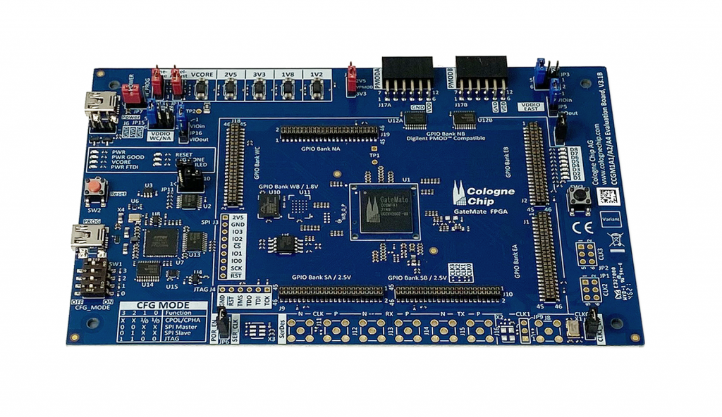
The GateMate™ FPGA Starter Kit offers an ideal entry point for embedded designers seeking a flexible, low-power platform based on the latest technology from Cologne Chip. It is designed for cost-sensitive projects and versatile applications.
- Evaluation board featuring the GateMate A1 or A2 FPGA
- Programmer adapter with a flat ribbon cable for custom PCBs
- USB cable
This comprehensive kit provides the essential tools to kick-start your FPGA development.
The fully open-source and license-free toolchain provides a complete flow for GateMate™ FPGAs — including synthesis, place & route, bitstream generation, and more.
Designed for usability and performance, the toolchain is lightweight, easy to install, and runs on all major platforms.

Build times are remarkably faster compared to traditional vendor tools, and the open nature of the ecosystem offers transparency, customization, and integration with a broad range of open-source tools.
Complete RTL-to-Bitstream Flow
GateMate™ FPGAs are supported by a streamlined open-source toolchain that includes:


openFPGALoader
Fast and versatile programmer with support for FTDI, RP2040 and various SPI flashes
Latest Builds
Get the latest builds directly from the official GitHub releases of the OSS CAD Suite:
🔗 Download Latest oss-cad-suite Builds (Windows, Linux, macOS, ARM)
These daily builds include all necessary tools (Yosys, nextpnr with GateMate support, openFPGALoader) pre-packaged for plug-and-play use.
💡Getting Started & Examples
With our Quickstart Guide, you can set up OSS CAD Suite in just a few minutes.
You also find a wide variety of examples in our Testcases Repository.
Need help getting started? Feel free to reach out via Contact Us. Whether you’re on Windows, Linux, macOS or an ARM64 based Linux device — we’re here to help you get building in minutes.
The Cologne Chip GateMateTM family addresses a complete range of system requirements. The following table compares all available devices:
| A1 ✅ | A2 ✅ | A4 🔜 | A9🆕 | A16 🆕 | A25 🆕 | |
|---|---|---|---|---|---|---|
| CPEs | 20,480 | 40,960 | 81,920 | 184,320 | 327,680 | 512,000 |
| Registers | 40,960 | 81,920 | 163,840 | 368,640 | 655,360 | 1,024,000 |
| Block RAM (20K/40K) | 64/32 | 128/64 | 256/128 | 576/288 | 1,024/512 | 1,600/800 |
| PLLs | 4 | 8 | 16 | 36 | 64 | 100 |
| SerDes (5G) | 1 | 2 | 4 | 9 | 16 | 25 |
| Multipliers | arbitrary | arbitrary | arbitrary | arbitrary | arbitrary | arbitrary |
| Max. single-ended IOs | 162 | 162 | 154 | up to 1,458 | up to 2,592 | up to 4,050 |
| Max. LVDS pairs | 81 | 81 | 77 | up to 729 | up to 1,296 | up to 2,025 |
| Package Options | Bare-Die Flip-Chip FBGA324 15×15 mm | Bare-Die Flip-Chip FBGA324 15×15 mm | Bare-Die Flip-Chip FBGA324 15×15 mm | Bare-Die Flip-Chip | Bare-Die Flip-Chip | Bare-Die Flip-Chip |
✅ In mass production and available from stock in volumes
🆕 In mass production and available as Bare-Dies (Flip-Chip)
28nm – Made in Germany
Manufactured using Globalfoundries advanced 28nm Super Low Power (SLP) process technology, GateMate FPGAs deliver good performance and energy efficiency. Produced in Germany, they ensure best quality and a robust supply chain at all times.

Innovative FPGA Architecture
GateMate’s architecture is built around an efficient 8-input LUT-tree, enabling complex logic functions with minimal resource usage. Integrated scalable multipliers and 8-input multiplexers provide enhanced arithmetic capabilities and flexible data routing.
Innovative Multi-Die Concept
Cologne Chip’s patented in-silicon die-to-die interconnects allow larger FPGAs to be cut from a single wafer and enables considerably more and faster connections between multiple dies in one package.


Instant-on Configuration
Experience near-instant FPGA readiness with GateMate’s ultra-fast configuration capabilities. Support for 100 MHz Quad-IO SPI, JTAG and a customizable internal interface ensures seamless integration and the flexibility to build proprietary configuration systems.
Bitstream Scrubber
This built-in mechanism, that continuously refreshes the configuration bits, enhances reliability and fault tolerance, making the devices well-suited for radiation-prone environments such as aerospace, medical, or high-altitude applications.


Easy Integration and Pin Compatibility
GateMate’s smallest BGA package with up to 9 GPIO banks simplifies PCB design with easy escape routability on just 2 signal layers. Pin compatibility across GateMate A1, A2 and A4 ensures seamless upgrades and design flexibility.
High-speed Serial Interface
The GateMate SerDes achieves line rates up to 5 Gbit/s. It features highly-configurable data paths (16/20-, 32/40- or 64/80-bit), 8B/10B encoding/decoding, automatic comma detection, RX clock data recover, TX emphasis control mechanisms and various tools for assessing the signal integrity in your environment.


Wide Temperature Range
GateMate FPGAs operate reliably across an extended temperature range from -40 °C to +125 °C. This makes them ideal for industrial, automotive, and other mission-critical applications requiring high thermal resilience.
Flexible Multipliers
Each logic cell features a compact 2×2 bit multiplier with direct interconnection to neighboring cells: This architecture enables arbitrary-sized multipliers at any position on the chip, optimizing designs for DSP and filter applications.


Open Toolchain and Ecosystem
GateMate FPGAs embrace open source innovation with support for powerful tools like Yosys for synthesis, nextpnr for place & route and openFPGALoader for programming. Additionaly, they integrate seamlessly into the LiteX SoC builder framework, enabling developers to leverage a rich ecosystem for efficient and flexible FPGA design.